In this tutorial, we will learn how to use GPIO pins of Pic microcontroller. We will see how to configure general purpose pins either as a digital input and digital output. For demonstration, we will use PIC18F452 microcontroller but you can also any other Microchip microcontroller also.
Pic Microcontroller GPIO Pins Introduction
The PIC18F452 microcontroller uses a number of input/output pins for connection with external devices. It has a total of 40 pins, out of which 34 can serve as input/output pins. These pins are grouped into five ports, which are Port A, Port B, Port C, Port D, and Port E. This article will teach you how to utilize the I/O ports of the PIC18F452 microcontroller.
PortA
Port A consists of seven pins named as RA0-RA6.
PortB
Port B consists of eight pins named as RB0-RA7.
PortC
Port C consists of eight pins named as RC0-RC7.
PortD
Port D consists of eight pins named as RD0-RD7.
PortE
Port E consists of three pins named as RE0-RE2.
GPIO Pins Configuration Registers
Each port has three registers for its operation. These registers are:
- TRIS register (data direction register)
- PORT register (reads the levels on the pins of the device)
- LAT register (output latch)
1. TRIS Register
TRIS is a data direction register. Setting the TRIS bit for the corresponding port determines the data direction (read or write) of the microcontroller. Each port has its own TRIS register. For example, to make Port A an output port, we can use the following code:
TRISA = 0; // making port as output port (write)To make a specific bit of the port as input or output, we can use the following code:
TRISA.F2 = 1; // configure PORTA pin RA2 as input2. PORT Register
The PORT register is to read the levels on the pins of the device and assign logic values (0/1) to the ports.
Input Mode of Port A
In the input mode of Port A, the status of the pins can be read by reading the PORTA register. First, we need to set the direction of data by setting the TRISA bit to 1, which makes the corresponding PORTA pin an input and puts the corresponding output driver in a Hi-Impedance mode. Example code:
TRISA = 1; // making port as input port (read)PORTA = 0xFF; // reading the status of the pins (input mode)Output Mode of Port A
In the output mode of Port A, we need to set the direction of data using the TRISA register and assign a value to the port for output. A write to the PORT register writes the data value to the port latch. Example code:
TRISA = 0; // making port as output port (write)PORTA = 0x03; // assigning high logic to RA0 and RA13. LAT Register
The LAT (Latch) register is associated with an I/O pin and eliminates the problems that could occur with read-modify-write instructions.
Latch Read
A read of the LAT register returns the values held in the port output latches instead of the values on the I/O pins.
Latch Write
A write to the LAT register has the same effect as a write to the PORT register. A write to the PORT register writes the data value to the port latch.
PORTA
Port A is a 7-bit wide, bi-directional I/O port. The corresponding Data Direction register is TRISA.
The following table mentions the function and features of each pin.
| Bit | Pin | I/O | Analog Input (AN) | TTL/ST | Function | Additional Features |
|---|---|---|---|---|---|---|
| 0 | RA0 | I/O | AN0 | TTL | ||
| 1 | RA1 | I/O | AN1 | TTL | ||
| 2 | RA2 | I/O | AN2 | TTL | VREF- | |
| 3 | RA3 | I/O | AN3 | TTL | VREF+ | |
| 4 | RA4 | I/O | TTL | T0CKI | ST, Open Drain | |
| 5 | RA5 | I/O | AN4 | TTL | SS, LVDIN | Multiplexed Inputs |
| 6 | RA6 | I/O | TTL | OSC2/CLK0 |
You can set the function of each pin by selecting the control bits in the ADCON1 register.
PORTB
Port B is an 8-bit wide, bi-directional port. The corresponding Data Direction register is TRISB.
The following table mentions the function and features of each pin.
| Bit | Pin | I/O | TTL/ST | Function | Additional Features |
|---|---|---|---|---|---|
| 0 | RB0 | I/O | TTL/ST | INT0 | |
| 1 | RB1 | I/O | TTL/ST | INT1 | |
| 2 | RB2 | I/O | TTL/ST | INT2 | |
| 3 | RB3 | I/O | TTL/ST | CCP2 | |
| 4 | RB4 | I/O | TTL | Interrupt on Change | |
| 5 | RB5 | I/O | TTL/ST | Interrupt on Change | ICSP enable pin |
| 6 | RB6 | I/O | TTL/ST | Interrupt on Change | Serial prog. clock |
| 7 | RB7 | I/O | TTL/ST | Interrupt on Change | Serial prog. data |
PORTC
Port C is an 8-bit wide, bi-directional port. The corresponding Data Direction register is TRISC.
The following table mentions the function and features of each pin.
| Bit | Pin | I/O | TTL/ST | Function |
|---|---|---|---|---|
| 0 | RC0 | I/O | ST | TMR1 oscillator output |
| 1 | RC1 | I/O | ST | TMR1 oscillator input, CCP2 |
| 2 | RC2 | I/O | ST | CCP1 |
| 3 | RC3 | I/O | ST | |
| 4 | RC4 | I/O | ST | SDI/SDA |
| 5 | RC5 | I/O | ST | SDO |
| 6 | RC6 | I/O | ST | TX/CK |
| 7 | RC7 | I/O | ST | RX/DT |
PORTD
Port D is an 8-bit wide, bidirectional port. The corresponding Data Direction register is TRISD.
The following table mentions the function and features of each pin.
| Bit | Pin | I/O | TTL/ST | Function |
|---|---|---|---|---|
| 0 | RD0 | I/O | ST/TTL | Parallel slave port bit 0 |
| 1 | RD1 | I/O | ST/TTL | Parallel slave port bit 1 |
| 2 | RD2 | I/O | ST/TTL | Parallel slave port bit 2 |
| 3 | RD3 | I/O | ST/TTL | Parallel slave port bit 3 |
| 4 | RD4 | I/O | ST/TTL | Parallel slave port bit 4 |
| 5 | RD5 | I/O | ST/TTL | Parallel slave port bit 5 |
| 6 | RD6 | I/O | ST/TTL | Parallel slave port bit 6 |
| 7 | RD7 | I/O | ST/TTL | Parallel slave port bit 7 |
PORTE
Port E is a 3-bit wide, bidirectional port. The corresponding Data Direction register is TRISE.
The following table mentions the function and features of each pin.
| Bit | Pin | I/O | Analog Input (AN) | TTL/ST | Function |
|---|---|---|---|---|---|
| 0 | RE0 | I/O | AN5 | ST/TTL | RD, parallel slave port bit 0 |
| 1 | RE1 | I/O | AN6 | ST/TTL | WR, parallel slave port bit 1 |
| 2 | RE2 | I/O | AN7 | ST/TTL | CS, parallel slave port bit 2 |
Pic Microcontroller Example to Use GPIO Pins
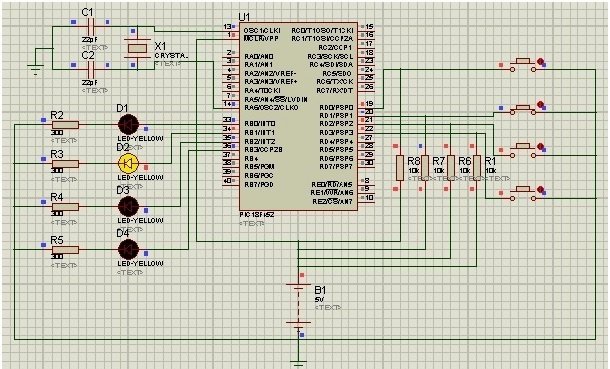
The provided circuit shows how to use the input/output ports of a PIC18F452 microcontroller for controlling LEDs based on the user’s input with push buttons.
Here’s a detailed explanation of the circuit:
- The circuit utilizes the PIC18F452 microcontroller, a popular microcontroller manufactured by Microchip. It has various input/output pins that can connect external devices.
- Four push buttons connect to the input pins of Port D of the microcontroller (RD0, RD1, RD2, and RD3). These buttons serve as user inputs and control the LEDs.
- Four LEDs are connected to the output pins of Port B of the microcontroller (RB0, RB1, RB2, and RB3). They indicate the status of the corresponding push buttons.
- Each push button is connected in a pull-up configuration, meaning it connects to the Vcc (5V) supply voltage via a resistor. The resistor pulls the pin of the microcontroller high when the button is not pressed and low when the button is pressed.
- Each LED is in series with a current-limiting resistor to control the current flowing through it. These resistors prevent the LEDs from burning out due to excessive current.
- The Proteus software simulates the circuit’s functionality. The provided code demonstrates how to read the state of the push buttons from Port D and write corresponding values to Port B, controlling the LEDs. The LEDs light up when the corresponding button is pressed and turn off after a one-second delay.
Overall, the circuit showcases a basic example of using the GPIO (General Purpose Input/Output) pins of the PIC18F452 microcontroller to control external devices based on user input.
Code mikroC for Pic
The code for this project is written in the MIKROC compiler and 8Mhz crystal is used in this project. If you do not know how to use MikroC for Pic, you can refer to these tutorials:
- How to Use “MikroC PRO for PIC” to Program PIC Microcontrollers
- Pic microcontroller programming in c using Mikroc Pro for PIC
void main()
{
    // Configure PORTD pins as inputs
    TRISD.F0 = 1; // 1st bit of PORTD as input
    TRISD.F1 = 1; // 2nd bit of PORTD as input
    TRISD.F2 = 1; // 3rd bit of PORTD as input
    TRISD.F3 = 1; // 4th bit of PORTD as input

    // Configure PORTB pins as outputs
    TRISB.F0 = 0; // 1st bit of PORTB as output
    TRISB.F1 = 0; // 2nd bit of PORTB as output
    TRISB.F2 = 0; // 3rd bit of PORTB as output
    TRISB.F3 = 0; // 4th bit of PORTB as output

    // Initialize PORTB to turn off all LEDs
    PORTB = 0x00; // All LEDs OFF

    do
    {
        // Check if the 1st switch is pressed
        if (PORTD.F0 == 0)
        {
            PORTB.F0 = 1; // Turn on the 1st LED
            Delay_ms(1000); // Delay for 1 second
            PORTB.F0 = 0; // Turn off the 1st LED
        }

        // Check if the 2nd switch is pressed
        if (PORTD.F1 == 0)
        {
            PORTB.F1 = 1; // Turn on the 2nd LED
            Delay_ms(1000); // Delay for 1 second
            PORTB.F1 = 0; // Turn off the 2nd LED
        }

        // Check if the 3rd switch is pressed
        if (PORTD.F2 == 0)
        {
            PORTB.F2 = 1; // Turn on the 3rd LED
            Delay_ms(1000); // Delay for 1 second
            PORTB.F2 = 0; // Turn off the 3rd LED
        }

        // Check if the 4th switch is pressed
        if (PORTD.F3 == 0)
        {
            PORTB.F3 = 1; // Turn on the 4th LED
            Delay_ms(1000); // Delay for 1 second
            PORTB.F3 = 0; // Turn off the 4th LED
        }
    } while (1); // Infinite loop
}
How Does Code Work?
Here’s an explanation of the code line by line:
void main()This line starts the main function, which is the entry point of the program.
{This opens the main function block.
    // Configure PORTD pins as inputs
    TRISD.F0 = 1; // 1st bit of PORTD as input
    TRISD.F1 = 1; // 2nd bit of PORTD as input
    TRISD.F2 = 1; // 3rd bit of PORTD as input
    TRISD.F3 = 1; // 4th bit of PORTD as input
These lines configure the pins of PORTD (RD0, RD1, RD2, and RD3) as inputs using the TRISD register.
    // Configure PORTB pins as outputs
    TRISB.F0 = 0; // 1st bit of PORTB as output
    TRISB.F1 = 0; // 2nd bit of PORTB as output
    TRISB.F2 = 0; // 3rd bit of PORTB as output
    TRISB.F3 = 0; // 4th bit of PORTB as output
These lines configure the pins of PORTB (RB0, RB1, RB2, and RB3) as outputs using the TRISB register.
    // Initialize PORTB to turn off all LEDs
    PORTB = 0x00; // All LEDs OFF
This line sets the initial value of PORTB to 0x00, turning off all LEDs connected to PORTB.
    do
    {
This line starts a do-while loop that will run indefinitely.
        // Check if the 1st switch is pressed
        if (PORTD.F0 == 0)
        {
            PORTB.F0 = 1; // Turn on the 1st LED
            Delay_ms(1000); // Delay for 1 second
            PORTB.F0 = 0; // Turn off the 1st LED
        }
This code snippet checks whether the first switch connected to RD0 is pressed. If it is, it turns on the first LED connected to RB0 for 1 second and then turns it off.
        // Check if the 2nd switch is pressed
        if (PORTD.F1 == 0)
        {
            PORTB.F1 = 1; // Turn on the 2nd LED
            Delay_ms(1000); // Delay for 1 second
            PORTB.F1 = 0; // Turn off the 2nd LED
        }
This block checks whether the second switch connected to RD1 is pressed. If it is, it activates the second LED connected to RB1 for 1 second and then deactivates it.
        // Check if the 3rd switch is pressed
        if (PORTD.F2 == 0)
        {
            PORTB.F2 = 1; // Turn on the 3rd LED
            Delay_ms(1000); // Delay for 1 second
            PORTB.F2 = 0; // Turn off the 3rd LED
        }
This code checks whether the third switch connected to RD2 is pressed. If it is, it turns on the third LED connected to RB2 for 1 second and then turns it off.
        // Check if the 4th switch is pressed
        if (PORTD.F3 == 0)
        {
            PORTB.F3 = 1; // Turn on the 4th LED
            Delay_ms(1000); // Delay for 1 second
            PORTB.F3 = 0; // Turn off the 4th LED
        }
This code checks whether the fourth switch connected to RD3 is pressed. If it is, it turns on the fourth LED connected to RB3 for 1 second and then turns it off.
} while (1); // Infinite loopThis line creates an infinite loop to keep checking the status of the switches and control the LEDs.
}This closes the main function block.
Video Demo
Conclusion
In conclusion, this tutorial has provided a comprehensive understanding of how to use GPIO pins of the PIC microcontroller. We have explored the different ports available on the PIC18F452 microcontroller, such as Port A, Port B, Port C, Port D, and Port E, and learned how to configure them as input or output.
Through the explanation of the GPIO pins’ configuration registers, namely the TRIS register, PORT register, and LAT register, we have gained insights into how to control the data direction, read input statuses, and write output values. These registers play a crucial role in managing the interaction between the microcontroller and external devices.
Related content:
- Getting Started With PIC Microcontrollers
- KEYPAD INTERFACING WITH PIC16F877A MICROCONTROLLER
- STEPPER MOTOR INTERFACING WITH PIC16F877A MICROCONTROLLER
- Interfacing a Servo Motor with PIC16F877A Microcontroller
- SERIAL COMMUNICATION USING PIC16F877A MICROCONTROLLER
- How to Use Pic Microcontroller Comparator Channels
- I2C Communication using PIC Microcontroller with Example Codes
hi malik,appreciate ur teaching. pls explain to my with example how I can write a message on a pin to be display on LCD .eg 5v on pin and it will Ind.power on and 0v on another pin Ind power off on lcd
#include “mcc_generated_files/mcc.h”
#define button1 PORTDbits.RD0
#define button2 PORTDbits.RD1
#define button3 PORTDbits.RD2
#define button4 PORTDbits.RD3
#define led1 LATBbits.LATB0
#define led2 LATBbits.LATB1
#define led3 LATBbits.LATB2
#define led4 LATBbits.LATB3
void main(void)
{
SYSTEM_Initialize();
TRISDbits.TRISD0 = 1;TRISDbits.TRISD1 = 1;TRISDbits.TRISD2 = 1;
TRISDbits.TRISD3 = 1;
TRISBbits.TRISB0=0; TRISBbits.TRISB1=0;TRISBbits.TRISB2=0;
TRISBbits.TRISB3=0;
while (1)
{
if(button1 == 0){led1=1; __delay_ms(1000),led1=0;}
if(button2 == 0){led2=1; __delay_ms(1000),led2=0;}
if(button3 == 0){led3=1; __delay_ms(1000),led3=0;}
if(button4 == 0){led4=1; __delay_ms(1000),led4=0;}
}
}
This is the correct code
with PIC18F45K22 micro controller
Thanks, Dear
your article is very related and to the point. I was finding out how to declare the single bit as input and output which I have found in your article. Thanks for this.
Thanks again.