AD9850 DDS Signal Generator Module is one of the small, low-cost boards to generate analog signals. This integrated board can be controlled through a microcontroller and can be digitally programmed using Direct Digital Synthesis Technology (DSS).

AD9850 DDS Signal Generator Module is equipped with an AD9850 IC, a powerful Oscillator of 125MHz, and a DSS synthesizer. It operates at a very low power supply, thus finding applications in many small self-assembly projects to produce square and sine waves.
This tutorial is a brief introduction to the AD9850 DDS Signal Generator Module and its specifications. The pin configuration, features, interfacing, and applications will also be discussed here.
AD9850 SGM Components
The AD9850 Signal Generator Module consists of the following components:

Crystal Oscillator: The module contains a crystal oscillator to provide clock and timing control for the Integrated Circuit.
Duty Cycle or Amplitude Adjustment: The module is provided to adjust the signals’ offset and pulse widths through the in-built potentiometer.
AD9850 IC: This integrated circuitry does all the processing. With the help of a powerful Oscillator and other components, it can output analog signal waves.
Power LED: The power LED is provided to indicate the status of the power supply.
AD9850 Pinout
The following diagram shows the pinout of the AD9850 DDS Signal Generator Module:
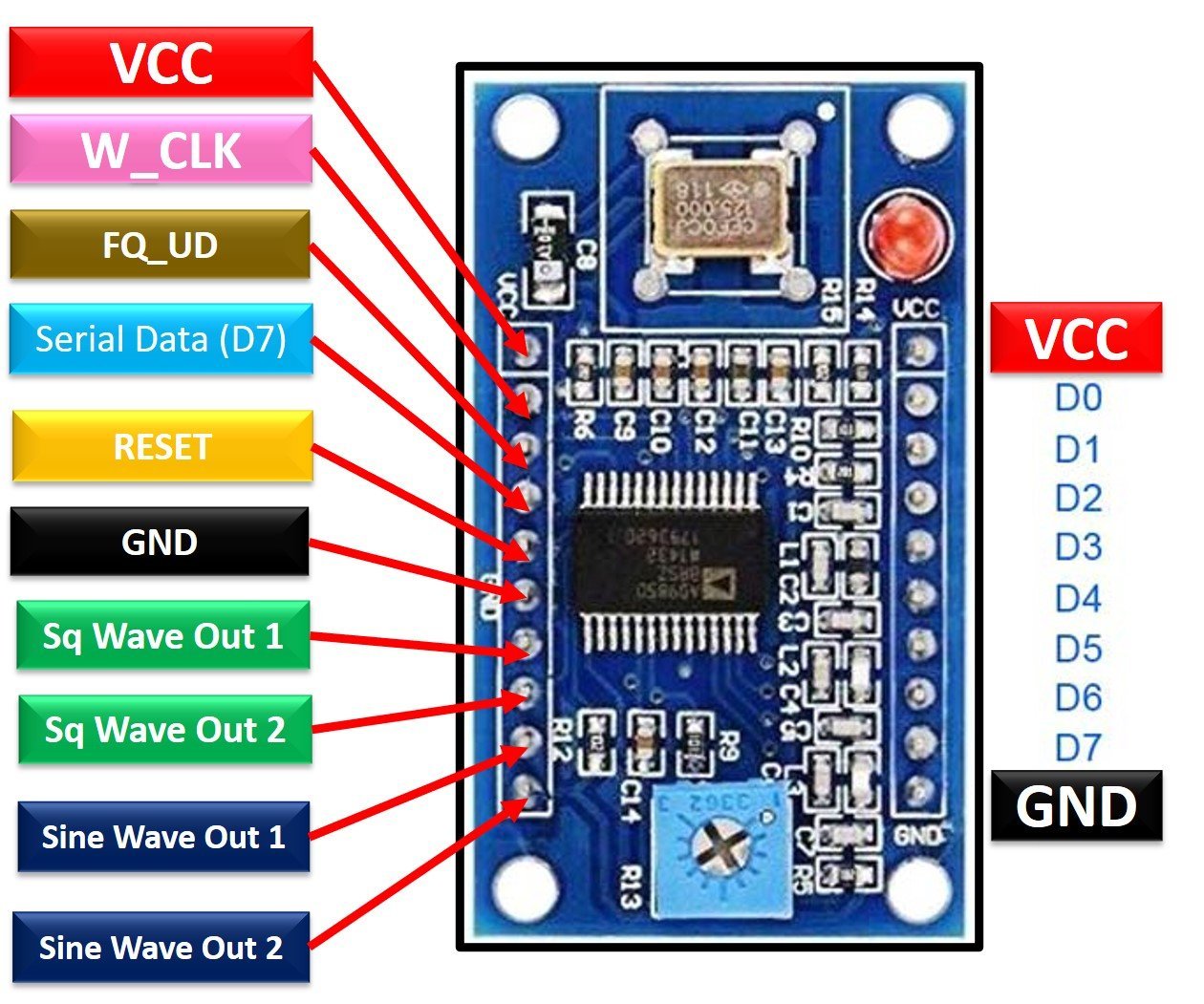
Pin Configuration
Let us discuss the pinout of the AD9850 Signal Generator Module. The pin configuration detail in tabular is mentioned below:
| Pin Name | Function |
|---|---|
| VCC | Supply pin |
| D0-D7 | Data input pin |
| GND | Reference potential pin |
| W-CLK | Word Load Clock pin |
| FQ-UD | Frequency Update pin |
| Data | Serial data input through D7 pin |
| Reset | Master reset pin |
| Sine-Wave 1 | DAC Current Output pin |
| Sine-Wave 2 | DAC Current Output pin |
| Square-Wave 1 | DAC Complementary Output pin |
| Square-Wave 2 | DAC Complementary Output pin |
- Input/Output pins: These are 8-bit data pins used to load data up to 32-bit frequency and 8-bit phase/control word. D7(MSB) also serves the purpose of loading a 40-bit serial data word.
- W-CLK: A Word Load Clock is used to synchronize and load words serially or through parallel transmission.
- FQ-UD: Frequency Update is used to update the frequency in the input data register when the clock has a rising edge. After updating, it reset the pointer to the word 0
- DATA: This pin is connected to the D7 input pin. It is used to load serial data.
- RESET: A master RESET is used to clear all the registers except for the IC’s input register by putting it into a HIGH state. Moreover, the outputs of DAC will be converted to Cosine 0 after some clocks.
AD9850 Features and Specifications
- Operating Voltage: 3.3 – 6 Volts
- Oscillator Frequency: 125 MHz
- Output Frequency: 0 – 40 MHz
- Operational Temperature: -40 – 850C
- Source/Sink Continuous Current: 0.005 Amperes
- DAC Current: 0.03 Amperes
- Power Dissipation(125 MHz, 5V): 380 mWatts
- Power Dissipation(110 MHz, 3.3V): 110 mWatts
Detailed Features
- DAC with Spurious Free Dynamic Range to specify the generator’s performance
- It contains a power-down function for a short boot time.
- Data transmission can either be parallel or serial.
- Power Dissipation depends on the power supply voltage.
- Four Analog signal outputs i.e., Sine-Wave 1, Sine-Wave 2, Square-Wave 1, and Square-Wave 2
- A comparator to generate less jittering in square wave output
- Direct Digital Synthesizer is based on CMOS Technology for better functionality and performance.
- A small high-performance module with a surface-mount package to be operated at industrial temperature
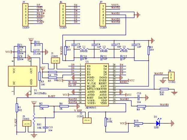
AD9850 SGM Schematic Diagram
The schematic of the module is provided to understand the connections which may turn helpful while repairing the module:
Interfacing AD9850 SGM with Arduino
The interfacing of the AD9850 Signal Generator Module is effortless and convenient. It can be connected to any microcontroller.
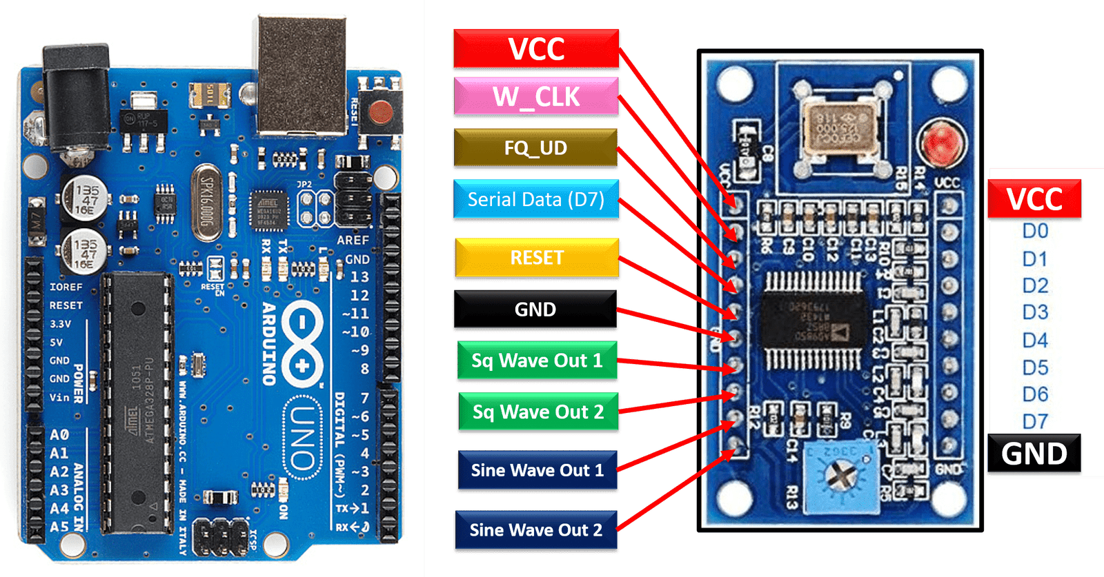
Now make connections with Arduino and AD9850 SGM according to this table:
| Arduino | AD9850 Module |
|---|---|
| +5V | Vcc |
| D13 | W_CLK |
| D8 | FQ_UD |
| D10 | Data |
| D9 | Reset |
| GND | GND |
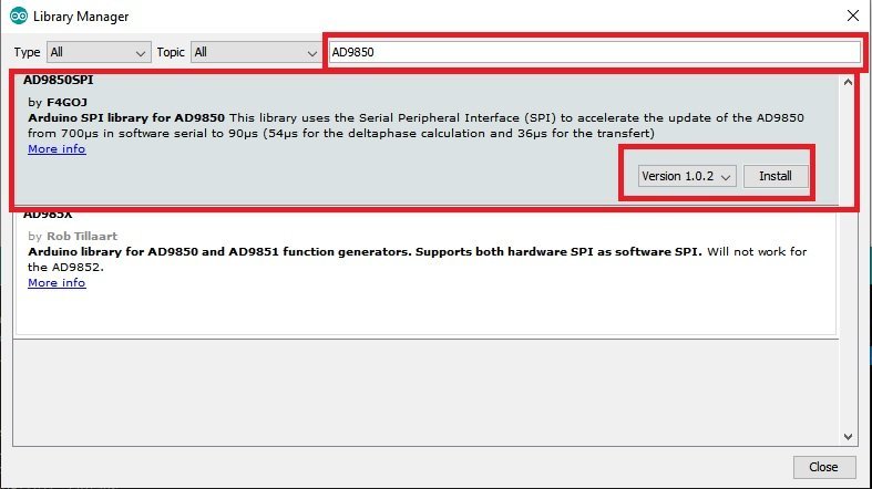
First, we need to install a library for AD9850 signal generator module in Arduino IDE. To install library, open Arduino IDE. Go to Tools > Library Manger.
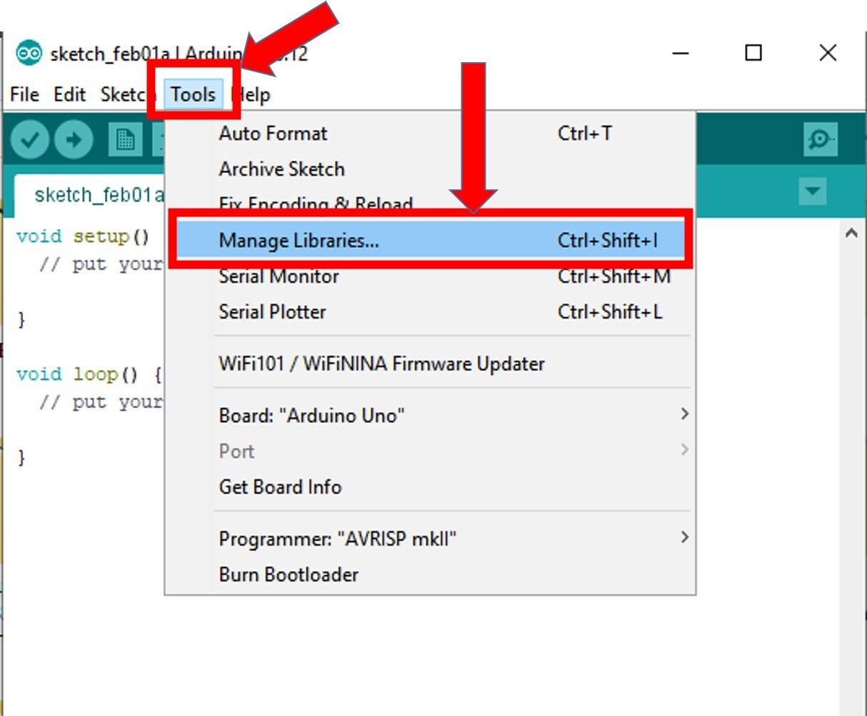
After that type AD9850 in search bar. You will get these options as shown in the picture. Select AD9850_SPI and click on install button.
Arduino Code
#include <AD9850SPI.h>
#include <SPI.h>

const int W_CLK_PIN = 13;
const int FQ_UD_PIN = 8;
const int RESET_PIN = 9;

double freq = 10000000;
double trimFreq = 124999500;

int phase = 0;

void setup(){
  DDS.begin(W_CLK_PIN, FQ_UD_PIN, RESET_PIN);
  DDS.calibrate(trimFreq);
}

void loop(){
  DDS.setfreq(freq, phase);
  delay(10000);
  DDS.down();
  delay(3000);
  DDS.up();
  delay(2000);
  DDS.setfreq(freq + 500, phase);
  delay(5000);
  DDS.down();
  while(1);
}
Compile the Arduino code and upload it to Arduino. As soon as the Arduino is powered, the AD9850 SGM will provide the frequency to the Square-wave out 1 and Sine-wave out 1. This can be observed visually through the Oscilloscope.
AD9850 Alternative Options
- AD9833 Signal Generator Module
- ICL8038 Signal Generator Module
Applications
- Waveform Generator
- Communication systems
- Clock based projects
- Analog-to-Digital Converters
2D Diagram
The following figure shows the 2d model of AD9850 DDS Signal Generator Module. It shows us the physical dimensions required when a PCB card is designed.

Related:
Intrested in your technic
I think DATA must be connected to Arduino D11, rather than D10 shown in the table above. Comments in the .cpp specify…and was necessary to make it work with my Uno. 🙂
That is right Mike. It works with Pin 11 on the Arduino and not Pin 10
I suppose I’m not the only person to notice that the schematic of the module in this guide is not the correct one – The pictures of the module show the current product, but the schematic is for the original version and the connectors are .totally different. 2 x 10 way headers rather than several smaller ones does get a bit confusing, but the options on the board are also reduced for simplicity – this may explain why there is no mention of their original purpose.
There also seems to be a difference of opinion of what the filter components should be – the crystal oscillator frequency sets the upper limit for the low-pass filter, which should be just above half the clock rate. i.e with a 125MHz crystal, the filter should pass up to around 70MHz.