24LC1026 is an external electrically erasable programmable Read-only memory introduced by Microchip. It supports a dual-directional I2C interface for data and address transfer among 4 devices. The benefit of 24LC1026 is that it is embedded with ESD protection and also wire protection. The memory is spacious and arranged in the form of 128K x 8 bits. It is an ultra-small, power-efficient device that has different clock frequencies depending on the input power voltage. The device can rewrite to one million write cycles and has a typical page write time of 3 milliseconds. The erase/write cycle of the device can be self-timed as well. It comes in two types of packages and is very reliable and space-efficient.
24LC1026 EEPROM is specially designed for personal applications extending from the Consumer level to the industry. This tutorial is a brief guide of 24LC1026 pinout, specifications, features, and applications.
24LC1026 Pinout
The chip is available in 8-pin PDIP, SOIC/SOIJ package. The following diagram shows the pinout of the 24LC1026 Serial EEPROM:
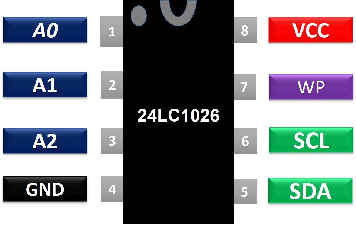
Pin Configuration
The pin configuration in tabular are detailed as below:
| Pin Number | Pin Name | Function |
|---|---|---|
| 1 | NC | Not Connected |
| 2 | A1 | User chip select pin |
| 3 | A2 | User chip select pin |
| 4 | VSS | Reference potential pin |
| 5 | SDA | Open-drain Serial Data line pin |
| 6 | SCL | Serial Clock line pin |
| 7 | WP | Write Protect pin |
| 8 | VCC | Positive Power supply pin |
Pin 2, 3 Address pins
The integrated EEPROM chip has two address pins. It serves the purpose of connecting multiple devices on a single bus. It has the capacity to connect 4 different devices at a time.
Pin 5, 6 I2C Interface
The 24LC1026 Serial EEPROM uses an inter-integrated circuit (I2C) interface for data transfer. It uses two pins i.e. SCL and SDA. SCL is responsible for data synchronization between this memory component and other devices. While bi-directional SDA is a transceiver that communicates addresses and data between EEPROM and other peripherals
Pin 7 Write Protect
The write protection prevents any mechanical data modification in the EEPROM.
When it is connected to VSS, it enables Write operations. When connected to VSS, the write operations are halted but read operations remain the same.
24LC1026 Specifications
- Operating Voltage: 2.5 Volts – 5.5 Volts
- Maximum Operating Voltage: 6.5Volts
- Operating Current: 5.0 mA
- Maximum Read Current: 450uA
- Write Current: 5mA
- Standby Current: 5uA
- Maximum Clock Frequency: 400 kHz
- Data Retention Time: >200 years
- Number of Write cycles: 1 million
- Typical Page Write time: 3msec
- Maximum Write Cycle time: 5msec
- Page Write Buffer: 128 Bytes
- ESD Protection: >400V
- operating temperature: -40°C to 85°C
- Package-Type: 8-pin PDIP, SOIC/SOIJ package
24LC1026 Features
- The memory device is based on low-power CMOS technology for fast processing.
- It can associate 1024K bits of serial data, internally arranged as 128K words of 8 bits each.
- 24LC1026 works on the I2C protocol for serial transmission and can connect up to 4 devices.
- It has an integrated mechanism to eradicate ground bounce produced by transistor switching.
- It has a Schmitt Trigger to filter the inputs to suppress inadmissible noise.
- Data Transfer Protocol in 24LC1026 is two-wired and supports a self-timed write/erase cycle.
- It is embedded with hardware wire protection to avoid mechanical data alteration.
- The module is a low-power, cost-effective, and highly durable device.
24LC1026 Timing Diagram
The EEPROM works on start-stop conditions and all the data communication takes place in between. The diagram is quite an explanation in itself.
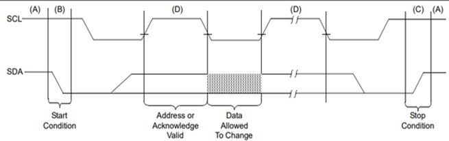
To start the transmission, SCL is pulled high and the SDA data line transits from high to low. After the start-up, the master device can transmit the information but as SCL is positive-edge triggered so the data line should be high and stable at that time. The data can only be varied when the clock is low. To terminate the transference, the SDA must be changed from low to high while SCL is high.
After the serial reception and transmission of 8-bit addresses and information, an acknowledge bit is sent to confirm that all the bytes are communicated.
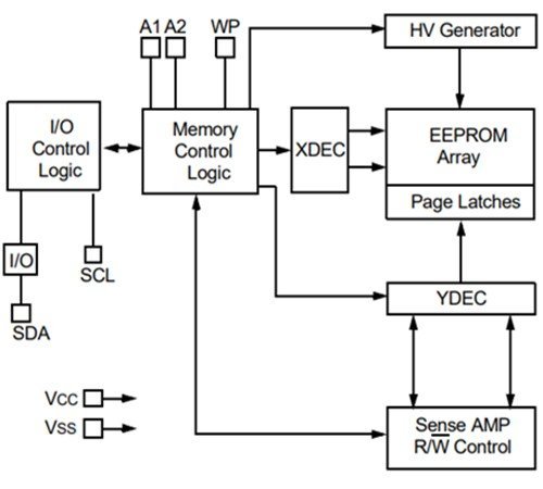
Block Diagram
The schematic diagram for a better conception of the arrangement of components of the Integrated Circuit of the 24LC1026 EEPROM is as shown:
Interfacing 24LC1026 EEPROM with Microcontroller
The following diagram shows the interfacing of the 24LC1026 EEPROM with any microcontroller which has I2C port.
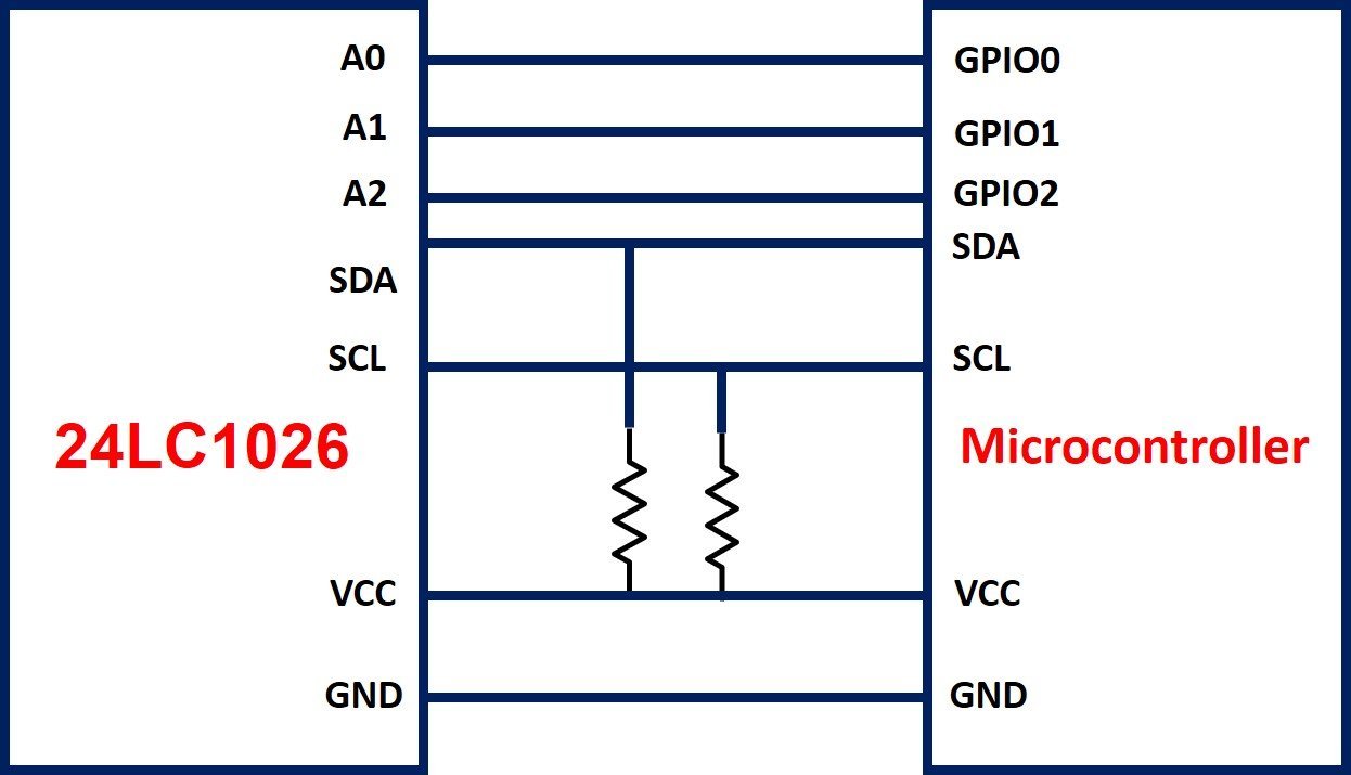
The I2C supporting microcontroller is connected to the external 24LC1026 EEPROM through SCL and SDA. The master-slave relation is carried out by these open-drain data lines. So they require pull-up resistors to avoid data loss. The address pins are sealed with any GPIO pins of the microcontroller unit if required. They are helpful to set the addresses when multiple devices are connected to a common microcontroller otherwise they are grounded.
The hardware WP is enabled when it is provided with voltage. It protects the whole memory array from data loss. To perform normal read and write functions, it must be kept low otherwise it allows data and address to be read only and forbids the write operations.
The communication is initiated by transferring the device address to the EEPROM which is followed by the memory address. After the allocation of the addresses, information is transmitted and stored at the specified location. Whenever data is needed to be read, requests are sent that contain the specified device and memory address. And the data is returned by the EEPROM.
Interfacing with Arduino
You can download Arduino libray for this EEPROM IC from here:
In the following tutorials, we have used different EEPROM IC’s to read and write data from EEPROM:
Alternate Options
- 24LC512 (equivalent)
- 25LC050
- 24C32
Applications
- Data Acquisition
- Audio electronics
- Data Storage
- Consumer products
- Industrial applications
- Communication systems
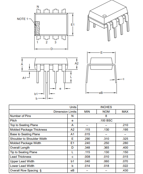
2D Diagram